TB-6328 · REV D · Technical newsheet
Machine Vision & InspectionDevice profile
Fraunhofer IPM Unveils Inline Optical QA: 3D Holography at 1 m/s
HoloTop Motion measures moving surfaces at up to 1 m/s with sub-2-µm lateral resolution and sub-µm axial reproducibility, no line stop needed.
By Nathan Brooks3 min read649 words
Features
- HoloTop Motion measures moving surfaces at feed rates up to 1 m/s without stopping the production line.
- Lateral resolution is better than 2 µm depending on lens; axial reproducibility is below 1 µm.
- F-Camera uses UV-induced fluorescence to detect and quantify organic contamination on electronic contacts.
- RAPID-LIBS resolves material transitions pulse by pulse during laser microvia drilling and feeds a real-time control signal to the laser.
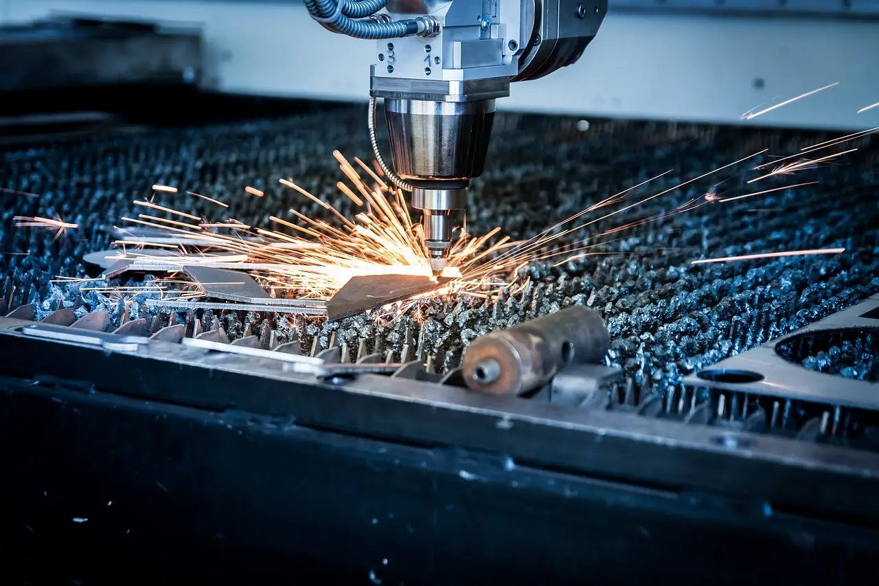
Fraunhofer IPM has demonstrated 3D topographic measurement of surfaces moving at feed rates up to one meter per second, with lateral resolution better than two micrometers and axial reproducibility under one micrometer. The sensor, called HoloTop Motion, is the first generation of digital holographic instruments that measures components without stopping or removing them from the production line, the institute says.
The development targets inline quality assurance in electronics manufacturing, where conventional metrology forces a stop-and-remove cycle that interrupts throughput. HoloTop Motion captures the surface strip by strip and combines the measurement data into a continuous topographic map. The institute positions the system for inspection of wafers, interposers and ball grid arrays, with the resolution figure dependent on the lens used.
What does motion-tolerant holography change?
Digital holography records the interference pattern between light scattered from the object and a reference wave, which lets the instrument reconstruct height information from a single exposure rather than scanning a point or line across a stationary target. That single-shot property is what removes the stop requirement. Strip-wise capture during continuous feed reconstructs the full surface topography of parts in motion, so inspection time collapses into the transport step itself. For wafer-level and advanced packaging inspection, where sub-micrometer axial reproducibility is the buying criterion, the claimed figures place the system in the same class as off-line profilometry while keeping the line running.
Fraunhofer IPM describes HoloTop Motion as a world first for this measurement mode.
Where does fluorescence inspection fit?
A second system, the F-Camera, addresses contamination on electronic contacts. Clean surfaces are a precondition for reliable welding, soldering, plugging and crimping connections, and for subsequent joining, coating or bonding processes. Residues of oils, greases, cleaning agents, lacquers or fluxes can impair component quality and function even at minute levels, the institute notes.
The F-Camera works without physical contact and integrates into the production cycle. UV light stimulates organic substances on the surface to fluoresce, making residues visible and quantifiable. The system captures the position, shape and extent of contaminants and defects, giving process engineers a measurable contamination signature rather than a pass/fail visual check.
The physics is straightforward: organic compounds absorb UV photons and re-emit at longer wavelengths, an effect absent from clean metal or ceramic surfaces. That contrast turns contamination inspection into an imaging measurement with quantified geometry, suitable for closing the loop on cleaning steps upstream.
How does RAPID-LIBS control microvia drilling?
A third development, RAPID-LIBS, tackles laser drilling of microvias, the structures that connect conductive layers of multilayer printed circuit boards. The process requires precise removal of insulating material without damaging the copper layer underneath. Fluctuating layer thicknesses make a fixed pulse count unreliable, according to the institute.
RAPID-LIBS analyzes the plasma that the laser itself generates during ablation. The system captures the material-specific emission spectrum and identifies in real time which material sits at the processing point. It resolves material transitions pulse by pulse and feeds the result back to the laser controller as a control signal, so the drill terminates each hole individually at the copper boundary rather than at a preset count.
Laser-induced breakdown spectroscopy is the underlying method: the ablation plasma emits lines characteristic of the elements present, and copper lines appear exactly when the insulation is gone. Because the probe is the processing laser, no separate illumination or sensor alignment is needed, and the measurement adds no cycle time.
What adoption question remains?
All three systems target inline integration, and Fraunhofer IPM presents them as production-ready inspection modules rather than laboratory instruments. The open question for electronics manufacturers is whether holographic, fluorescence and LIBS-based inspection can hold their specified accuracy inside real lines, with vibration, thermal drift and variable part carriers, at the throughput figures quoted. The institute publishes further details at www.ipm.fraunhofer.de.
via ipm.fraunhofer.de (Original)
Filed under
- inline-optical-inspection
- digital-holography
- fluorescence-imaging
- laser-induced-breakdown-spectroscopy
- electronics-manufacturing
More from Nathan Brooks
Show full bio
Staff writer covering people, launches and day-to-day practice in Instruments, test and measurement at Testbench Report.
87 articles
Application notes
- OMNIVISION Adds Two Global Shutter CMOS Sensors for Industrial Vision
- Wireless 3D Scanner Replaces Fixed Metrology at Fabricator TBI
- ETEL's METIS HP Brings Full Air Bearing Planarity to Semiconductor Scan Stages
- Machine Vision System Targets Micro-Defects in 3D-Printed Parts
- Robotic AI Metrology Hits 32 µm Accuracy on Blind Holes