TB-7860 · REV F · Technical newsheet
Test & MeasurementDevice profile
Korean Chip Test Equipment Maker Plans Design Center in Daegu
Korea's top chip test equipment maker will build a design center in Daegu, moving ATE development beyond Seoul toward regional engineering talent and fab-adjacent demand.
By Olivia Hart3 min read556 words
Features
- South Korea's leading chip test equipment maker will build a design center in Daegu, per the Seoul Economic Daily.
- The plan covers a design center, not a volume production facility; investment, headcount, and timeline figures were not disclosed.
- The move places ATE development outside the Greater Seoul semiconductor equipment corridor, aligning with policy pushing chip R&D to regional hubs.
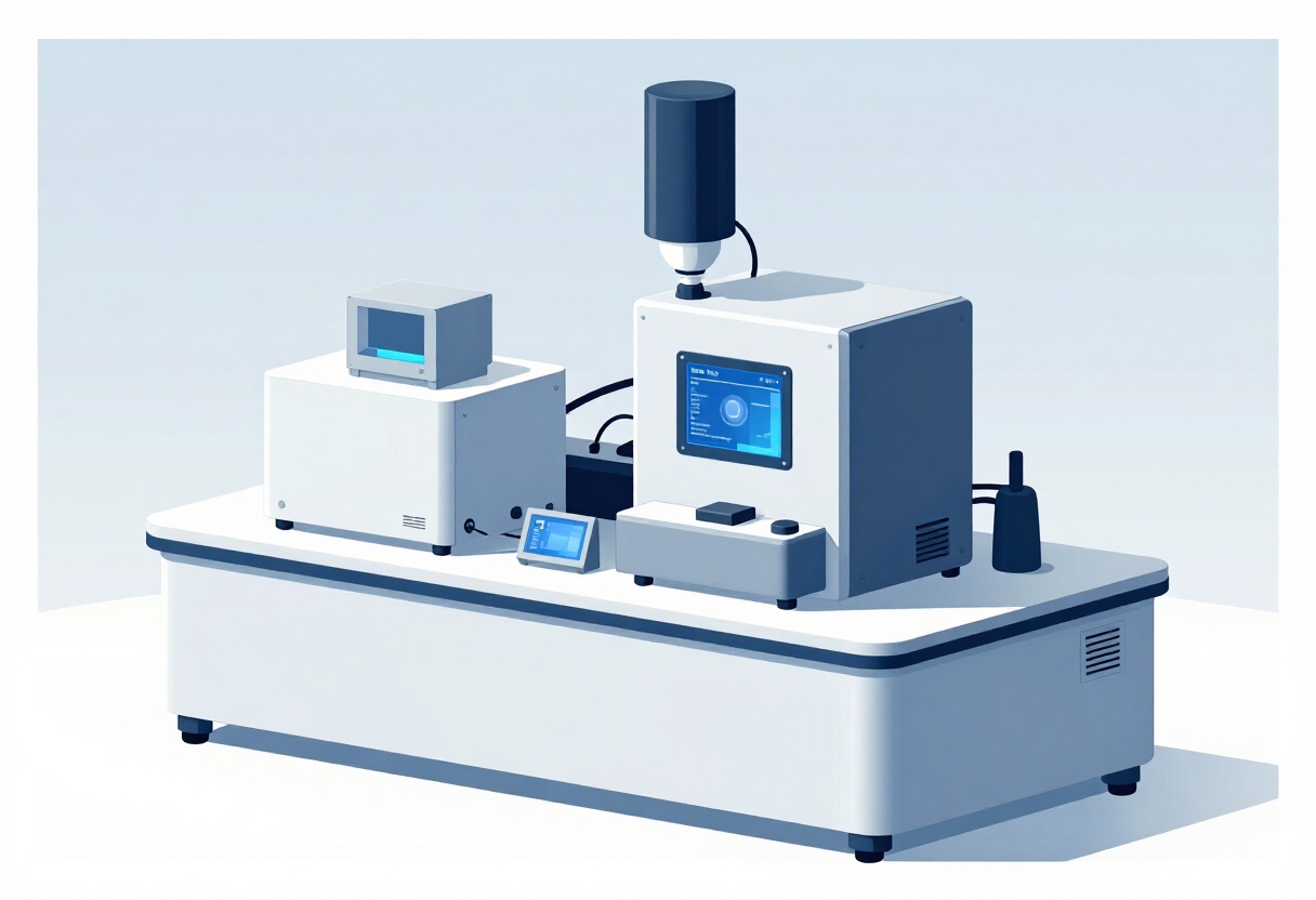
South Korea's leading domestic semiconductor test equipment maker will build a design center in Daegu, according to a report by the Seoul Economic Daily. The announcement shifts a meaningful piece of the country's automatic test equipment (ATE) engineering base out of the Greater Seoul corridor and into a metropolitan area better known for consumer electronics and display manufacturing than for front-end instrumentation development.
The reported plan centers on a design center — not a volume production plant. For test equipment vendors, that distinction matters. ATE roadmaps live or die on silicon-to-system integration work: pin electronics, timing ASICs, DSP-based measurement channels, and the software stacks that tie instruments to semiconductor device test specs. A design house in Daegu signals that the company intends to develop, not merely assemble, next-generation test platforms at the site.
Daegu offers the vendor a specific practical advantage: proximity to regional universities and engineering talent pools that cost measurably less to retain than equivalents in Seoul or Gyeonggi Province, where most of Korea's semiconductor equipment ecosystem — including the supplier clusters around Samsung's Hwaseong and Pyeongtaek fabs — concentrates. Locating design work roughly 240 km southeast of that corridor gives the company access to graduates from Daegu's engineering universities while keeping it inside the domestic supply chains it already serves.
The move also tracks a broader pattern in Korean industrial policy. Central and regional governments have spent the past several years pushing semiconductor design, packaging, and equipment R&D toward provincial hubs, in part to relieve the capital region's congestion and in part to seed test and measurement capability where large device makers plan packaging and back-end capacity. A design center from the country's top chip test equipment maker fits that template exactly: it puts high-value instrumentation engineering where policymakers want deepened fab-adjacent expertise.
What the report does not yet specify is equally telling. The Seoul Economic Daily item carries no figures for investment size, headcount, floor area, or a construction and commissioning timeline. Nor does it identify which product lines the Daegu center will design — whether system-level test hardware for SoCs and memory, wafer-level probe instrumentation, or board-level test modules. Buyers and process engineers tracking this vendor should treat the announcement as a capability-intent signal rather than a datasheet revision: until the company publishes scope figures, any judgment about delivery schedules for next-generation testers rests on inference, not specification.
For the domestic ATE market, the competitive stakes are concrete. Korea's device makers depend heavily on U.S. and Japanese tester suppliers for advanced logic and memory final test; a domestic vendor with a dedicated design center widens the local engineering base that device makers can call on for custom instrumentation, faster application engineering, and tester hardware closer to home. Each added design site compounds that advantage only if it ships product — which returns the question to execution.
The development raises a straightforward adoption question for Korean semiconductor manufacturers: will a locally designed, Daegu-engineered test platform earn qualification on advanced-node production lines, or will the center's output remain confined to supporting roles while imported ATE retains the performance-critical sockets? The answer will arrive not with the groundbreaking but with the first calibrated system that passes correlation on a production test floor.
via Google News: Oscilloscopes and test equipment (Source)
Filed under
- ate
- semiconductor-test
- korea
- design-center
- daegu
More from Olivia Hart
Show full bio
Market editor covering media and advertising at Testbench Report.
33 articles
Application notes
- FPGA Lead Times Hit 52 Weeks as Component Shortfall Bites Korean Test Equipment Makers
- Aemulus and Samsung Electro-Mechanics Move Test Collaboration Into Commercial Supply
- AI Chip Demand Drives Record Profits for Taiwan Test Equipment Makers
- Test Equipment Makers Vie for SK Hynix P&T7 Orders Up to 400 Billion Won
- Industrial Physics Acquires Vitrek, Consolidating Test Equipment Under KKR